Power Inverter Hardware
The Atinverter V2 power inverter is based on a single phase PWM inverter topology that is software-configurable for either 50Hz or 60Hz output. Pulse-width modulation (PWM) signals are generated by the ATMEGA328P using its hardware PWM pins. This signal is conditioned by a pair of gate drivers before being delivered to the H-bridge topology which converts the control signals into power signals. The resulting waveform is passed through a symmetrical LC filter, rendering a clean 50Hz or 60Hz sinusoidal output for delivery to the load.
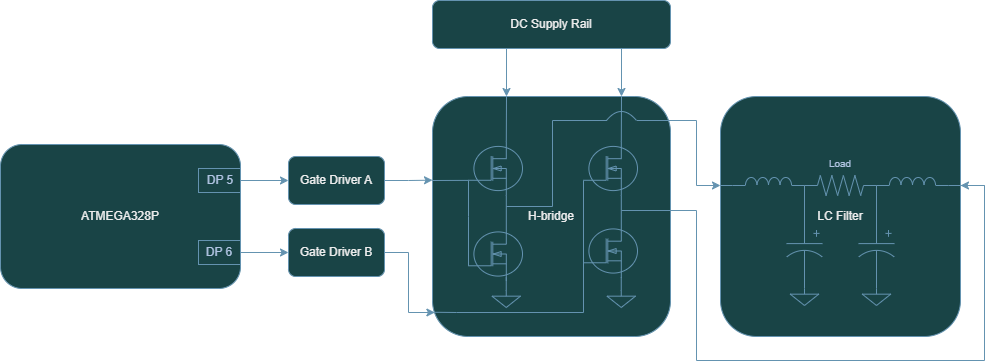
While the majority of the inverter architecture was carried over from the original Atinverter V1 design, two key hardware modifications were introduced in this iteration:
- Reduced bootstrap capacitor size: Decreased from 4.7 µF to 1 µF to limit inrush current and enhance switching efficiency.
- Higher gate drive voltage: The MOSFETs are now driven at a gate-to-source voltage of 12V instead of 5V, significantly improving conduction efficiency and reducing switching losses.
As most of the design was previously developed in the Atinverter V1 iteration, a detailed reference can be found in [citation]. Nonetheless, a brief description of each stage of the power inverter is covered.
〰️ PWM Generation
The power inverter operation is catalyzed by the PWM generation from the ATMEGA328P. This MCU generates pulse-width modulated (PWM) square waves at a frequency of 31,372Hz that, when combined with an appropriate switching circuit and filtering stage, can approximate the output of a 50Hz or 60Hz pure sine wave power inverter.
While there are other simpler approaches that can be employed to achieve inversion, such as square wave or modified square wave inverters, this one achieves higher levels of waveform fidelity. In other words, this modulation technique allows our output waveform to behave and appear more like a real sine wave.
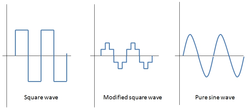 Source: Different Types of AC signals Produced by Inverters
🧠 Gate Drivers
The next stage in the power signal chain is the gate driver circuit. It performs two main tasks:
- Enabling high-side transistor drive capability in H-bridge through a bootstrap circuitry by level shifting the low-voltage PWM signals from the ATMEGA328P to higher voltages
- Enhance current delivery to the power transistors by sourcing gate drive current from an external supply, enabling rapid charging and discharging of gate capacitance for efficient switching.
🔁 H-Bridge Topology
Being composed of 4 power transistors that complimentarily switch at a specific frequency, the H-bridge topology is a conventional design that is widely implemented in many pure sine wave inverters. This design enables the connected load to experience a positive and negative voltage swing solely based on switching states, effectively eliminating the need for a negative supply rail. This dual-polarity effect is what allows for the production of a full AC swing across the load and is achieved by PWM control signals as well as only one DC supply.
🔉 LC Filter
Prior to delivering the power to the load, a low pass filter stage is employed to:
- Remove high frequency content, especially the switching frequency of the PWM signals.
- Preserve the fundamental frequency of interest. In our case, our PWM-based inverter is designed for 50 or 60Hz.